

For most of the last three years, public discussion of AI infrastructure centered on training: which lab had the largest cluster, how many GPUs went into a foundation model run, and how long that run took. That framing is increasingly out of date. Hyperscaler capital expenditure has continued to climb through 2026, but the workload consuming the majority of deployed GPU-hours at Microsoft, Google, Amazon, and Meta is no longer pretraining — it is inference.
Cloud providers now report that serving live traffic to deployed models, not training the next one, is where the bulk of AI-related compute cycles are spent and where AI revenue is actually collected. Training runs are episodic; inference runs continuously, twenty-four hours a day, against unpredictable user demand.
This shift changes what “good hardware” means. A chip optimized for training is judged on sustained matrix-multiply throughput across thousands of GPUs over weeks. A chip optimized for inference is judged on a different set of constraints entirely: how quickly it returns a first token, how consistently it holds latency under load, how much memory it has for model weights and key-value cache, and — ultimately — how many dollars it costs to generate a million tokens.
The NVIDIA B200, the flagship of the Blackwell generation, is frequently described in training-benchmark terms: FLOPS, MFU, time-to-train. This article deliberately sets that framing aside. It analyzes the B200 as a production inference system — not a chip in isolation, but the full stack of memory, power, cooling, networking, and software required to serve models at scale.
The central argument is that the B200 is best understood as an inference economics device: its architectural choices (memory bandwidth, memory capacity, FP4 precision) are aimed squarely at reducing the cost of serving tokens, and the deployment decisions around it (form factor, cooling, cluster design) are inference decisions as much as they are hardware decisions.
The NVIDIA B200 Architecture: What Changes for Inference
Memory bandwidth as the binding constraint
Large language model inference is, for most of its duration, memory-bandwidth-bound rather than compute-bound. During autoregressive decoding, the GPU generates one token at a time, and for each token it must read the model’s entire parameter set (plus the growing key-value cache) from high-bandwidth memory (HBM) into the compute cores. The arithmetic per token is comparatively small; the data movement is not.
Consider a 70-billion-parameter model running at 16-bit floating-point (FP16) precision. Each parameter occupies 2 bytes, so reading the full weight set once requires moving roughly 140 GB of data. On a GPU with 8 TB/s of memory bandwidth—the NVIDIA B200’s rated figure—that read alone takes on the order of 17-18 milliseconds, assuming the transfer approaches peak bandwidth in practice. This establishes a floor on per-token decode latency for a single request at batch size one, before accounting for compute time, kernel launch overhead, or network transfers.
It is also why raw compute throughput, typically measured in Floating-point Operations Per Second (FLOPs), is a misleading way to compare inference hardware: a chip can have enormous matrix-multiply capacity and still be idle, waiting on memory, if bandwidth cannot keep up with how fast weights need to be re-read. This is the core reason NVIDIA’s own inference speedup claims for B200 — on the order of a mid‑teens multiple over H100 when using native FP4 and Blackwell architectural optimizations — stem primarily from increases in memory bandwidth and lower‑precision formats
192GB HBM3e: what fits on one GPU
Memory bandwidth determines inference throughput; memory capacity determines how much model state can fit on a single GPU before sharding becomes necessary. NVIDIA’s DGX B200 Systems documentation lists the B200 configuration at 180 GB per GPU, while Epoch AI lists 192 GB of HBM3e. This analysis uses the 192 GB figure. Compared with 80 GB on the H100 and 40–80 GB on the A100, that represents roughly a 2.4× increase in HBM capacity. It pushes the sharding threshold higher — the point at which a model must be split across GPUs — and can reduce serving complexity for a wide range of production model sizes.
In practice, a 70B-parameter model at FP16 (~140 GB of weights, before KV cache) fits on a single B200 with headroom for concurrent requests. On an 80 GB H100, that same model requires aggressive quantization or Tensor Parallelism (TP) across at least two GPUs. Each additional GPU in the serving path adds synchronization overhead, kernel launch latency, and operational complexity — turning a 1-GPU problem into a multi-GPU problem with a lower effective utilization ceiling.
At 8-bit floating-point (FP8) precision, models around 150B parameters can theoretically fit within the B200’s 192 GB of HBM3e, although practical single-GPU deployment depends on the KV cache and serving overhead. At 4-bit floating-point (FP4) precision, substantially larger Mixture of Experts (MoE) architectures can potentially fit within a single GPU’s memory. This raises the sharding threshold further, widening the range of models that can avoid distributed serving entirely.
Very large frontier-scale models still require multi-GPU clusters regardless of precision. But for a wide swath of production workloads, B200 ensures that the primary operational constraint shifts from inter-GPU coordination back to raw compute and memory bandwidth. This simplifies capacity planning and improves fleet utilization, because fewer nodes are tied up managing the overhead of sharded models.
For an in-depth exploration of the memory-bandwidth bottleneck that governs B200 inference throughput, see Why HBM Has Become the Most Valuable Component in AI Hardware
FP4 precision: the real lever for cost per token
FP4 is where most of the NVIDIA B200’s inference economics story concentrates. Reducing weight and activation precision from FP8 to FP4 roughly halves the bytes that must move through memory per token, which — given that inference is bandwidth-bound — translates fairly directly into throughput gains, not just storage savings. NVIDIA’s second-generation Transformer Engine and NVFP4 Tensor Cores are built to make this precision drop usable in production rather than purely experimental.
However, quantizing to 4-bit precision reduces numeric headroom and can degrade quality, especially for numerically sensitive workloads or models not prepared for low-precision serving. Production teams mitigate this using calibrated block-scaled FP4 formats such as NVIDIA’s NVFP4, optionally applying Quantization-Aware Training (QAT) where needed, and using selective mixed precision — keeping a small number of sensitive computations (for example, important attention blocks or specific layers) at FP16 or FP8 while running most computation at FP4.
These accuracy mitigations only help if the serving stack actually runs the custom NVFP4 kernels (NVIDIA’s own co-design results show that generic FP4 kernels lose almost all of NVFP4’s quality benefit). Today, the software stack is functional but still maturing. TensorRT-LLM’s and vLLM’s Blackwell code paths are increasingly usable, and vLLM has been adding Blackwell-oriented kernels and attention-backend support, alongside broader production-serving features such as FP4 paths where available, KV-cache offloading, and speculative decoding.
FP4 kernel enablement has generally appeared first in datacenter Blackwell stacks — B100/B200-class SM100 GPUs and NVIDIA CUTLASS/TensorRT-LLM paths — ahead of broader consumer-SKU enablement. The practical implication is that “Blackwell support” is not monolithic: FP4 throughput, accuracy, and kernel coverage should be verified against the exact GPU SKU, driver, and inference-framework version.
NVLink 5: when it matters and when it does not
As mentioned in the NVIDIA Blackwell Architecture Technical Brief, the B200 features fifth-generation NVLink, offering 1.8 TB/s of bidirectional bandwidth per GPU. Given the 192 GB capacity, this bandwidth pays off mainly in multi-GPU configurations: a model that fits entirely within a single B200’s memory generally does not need NVLink. NVLink matters when models must be sharded across GPUs — either due to size or to reduce latency via tensor parallelism.
Here, fast interconnects minimize the communication overhead that would otherwise erode parallelism gains. In practice, the NVLink premium on systems like HGX or GB200 is only worth paying if the workload actually requires cross-GPU coordination.
For a complementary analysis of the compute-capacity dynamics shaping GPU procurement decisions today, see our deep-dive on AI Compute Constraint: Why GPUs and Infrastructure Now Define Artificial Intelligence.
Deployment Reality: The Physical System
Power and cooling
The NVIDIA B200 carries a base thermal design power (TDP) of 1,000 W per GPU — up from 700 W on the H100. At the density of a fully populated rack, this power figure makes cooling a primary deployment constraint, but the appropriate solution depends heavily on form factor.
For B200 SXM/HGX systems (eight-GPU baseboards), air cooling remains a viable and operational choice. A recent tour of Lambda’s multi-thousand-GPU Supermicro HGX B200 cluster in Columbus, Ohio — housed at Cologix and documented by Serve The Home — showed these servers operating in a fully air-cooled environment using high-capacity server-level heat sinks and facility-scale heat exchangers. Air cooling offers a meaningful speed-to-deployment advantage: HGX B200 servers can be brought online faster than facilities that must be retrofitted for liquid distribution. For many inference clusters, this makes air cooling the pragmatic near-term choice.
For GB200 NVL72 rack-scale systems, liquid cooling is physically mandatory. Packing 72 GPUs into a single coherent domain requires a density that air cooling cannot achieve — there is insufficient physical space for the requisite airflow, and the NVLink spine cabling would span distances too long to maintain signal integrity without the compact form factor that liquid cooling enables.
The industry trajectory favors liquid cooling: it is widely expected to become standard for new AI cluster builds within the next 18 months, and it enables higher rack density than air. But for a B200 inference deployment today, the decision is not whether to adopt liquid cooling, but which form factor to adopt. Teams without existing liquid-cooled facilities need not rule out B200; they can deploy HGX B200 in air-cooled environments and reserve liquid-cooled NVL72 systems for the specific frontier-scale workloads that justify the density.
Form factor decisions
Three distinct ways to deploy Blackwell-generation compute for inference, in increasing order of integration and cost:
- Standard HGX nodes (B200 SXM): Discrete GPU baseboards, typically 8 GPUs per node. The most flexible option — supports both air-cooled and liquid-cooled facilities and allows for incremental, node-level scaling within existing data center power envelopes.
- Integrated CPU-GPU nodes (GB200 Superchip): One Grace CPU paired with two B200 GPUs over a coherent 900GB/s NVLink-C2C interconnect. Typically requires liquid cooling due to high thermal density. Useful when workloads benefit from unified CPU-GPU memory or heavy preprocessing without explicit data copies.
- Rack-scale systems (GB200 NVL72): A liquid-cooled rack acting as a single logical GPU with 72 GPUs in one NVLink domain. Justified for frontier-scale model inference or massive context windows that require the 130TB/s aggregate bandwidth provided by the NVLink Switch System.
For inference specifically, the NVL72 is frequently more system than the workload requires. Independent analysis from Signal65 (SemiAnalysis) argues that the economics of inference favor smaller, localized compute domains over monolithic rack-scale systems for most production workloads.
Its value proposition is built around enabling very large models — hundreds of billions of parameters and up — to run as though they were on one enormous GPU, with the full 72-GPU NVLink domain acting as a unified memory and compute pool. That is a training-and-frontier-inference use case.
A team serving a 70B or smaller model, even at meaningful request volume, generally does not need a 72-GPU coherent domain — a handful of 8-GPU nodes, load-balanced behind a router, will serve the same traffic at a fraction of the capital commitment and with far more deployment flexibility.
The threshold where NVL72 becomes justified for inference is roughly where a single logical model instance exceeds what a small number of NVLink-connected GPUs can hold and serve within acceptable latency — typically frontier-scale models (400B+ parameters, especially large MoE architectures) or workloads requiring extremely large aggregate KV cache pools for very long context windows.
Networking requirements follow directly from these form-factor choices. As Signal65 notes, inference favors architectures where communication is localized. Unlike training — which demands sustained, high-bandwidth all-to-all communication across the entire cluster — inference traffic is largely request-scoped: a given request is served by a single GPU or a small NVLink-connected group of GPUs, with inter-node traffic limited to load balancing and request routing.
For most enterprise models, the massive cross-node bandwidth of an NVL72 exceeds what typical inference traffic patterns require. This means many B200 inference clusters can operate efficiently on Ethernet-based networking (including RoCE) rather than InfiniBand, trading fabric performance for lower cost and simpler operations — a tradeoff that is rational for inference but seldom for large-scale training.
The Software Stack for Production
Hardware capability only becomes production throughput through the serving software layer. The two dominant open frameworks — vLLM and NVIDIA’s TensorRT-LLM — have both added Blackwell-specific code paths, but with different maturity profiles.
TensorRT-LLM generally has earlier support for new hardware features like NVFP4 quantization, at the cost of a steeper integration process. vLLM has closed the gap over the course of 2026, adding FP4 support, an optimized attention backend, KV cache offloading, and speculative decoding.
Continuous batching — dynamically adding and removing requests from an in-flight batch — remains the standard technique both frameworks use to keep GPU utilization high, and is largely what makes the memory-bandwidth economics described in Section 2 achievable in production rather than only in benchmarks.
The operational metrics that matter for judging a production deployment are specific and worth naming explicitly:
- TTFT (Time To First Token): how long a user waits before any output appears, dominated by prefill compute over the input prompt.
- TPOT (Time Per Output Token): the steady-state generation rate once streaming begins, dominated by the memory-bandwidth-bound decode loop described earlier.
- P99 latency: tail latency under real, bursty load — often the metric that determines whether a deployment meets its service level agreement (SLA).
- Throughput under load: aggregate tokens per second the cluster sustains at a given concurrency level, which determines cost per token.
These metrics are not merely theoretical. Production load testing by the Cloud Native Computing Foundation demonstrates how they degrade under burst conditions: without autoscaling, TTFT can spike an order of magnitude above baseline and P99 end-to-end latency can extend to minutes, while throughput hits an inflection point beyond which additional concurrent load yields no additional throughput but rapidly worsens latency. This behavior is why continuous batching and autoscaling logic — not just raw hardware bandwidth — determine whether inference economics hold in production.
It is worth being direct about software maturity as a deployment risk. NVIDIA B200 support across the open-source inference ecosystem, while functional, is newer and less battle-tested than the equivalent H100 support that has had roughly two additional years of production hardening.
Teams evaluating B200 for production should expect to budget engineering time for kernel-level debugging, dependency version pinning (CUDA, PyTorch, and framework versions must align precisely), and validation of quantized model quality — not simply a drop-in hardware swap.
TCO and Economics: The Core Analysis
Cost-per-token analysis
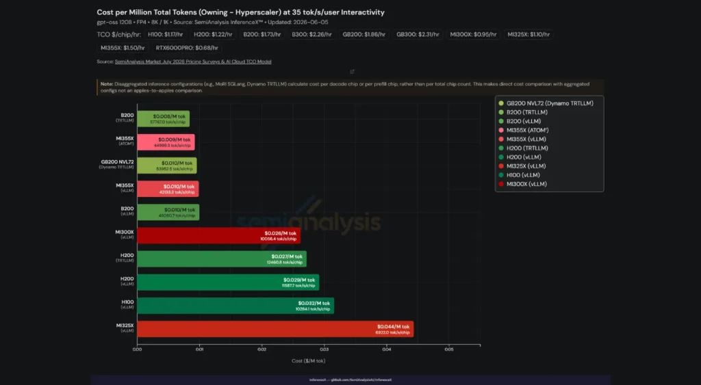
The headline economic claim around B200 inference cost comes from recent SemiAnalysis InferenceX benchmarks (August 2026) for GPT-OSS-120B-class models. Under optimized conditions, B200 systems deliver approximately $0.008–$0.010 per million tokens, depending on the serving framework — roughly $0.008 with TensorRT-LLM and $0.010 with vLLM. Against an H100 running vLLM at approximately $0.032 per million tokens under equivalent conditions, the improvement is roughly 3.2× to 4×.
Source: Semianalisys InferenceX
These figures are specific to a 120B-parameter model class and assume high utilization. They replace earlier industry estimates that placed H100 inference costs substantially higher. The gap is real but narrower than some headline claims: it comes from compounding higher memory bandwidth, larger memory capacity, and FP4 precision, not from any single architectural leap.
Utilization matters enormously. A cluster running at 30 percent utilization will show a cost-per-token figure several multiples worse than one sustained near 80–90 percent, regardless of hardware generation. Treat the ~3.2× figure as a realistic ceiling under favorable, well-tuned conditions, not a default outcome.
For a deeper treatment of the TCO framework and depreciation logic underpinning this analysis, see Why AI Cost Keeps Rising: Understanding the Economics of AI Infrastructure.
Cloud rental vs. on-prem
NVIDIA B200-class cloud pricing has been volatile through 2026 as supply has ramped. As of mid-2026, published on-demand rates span roughly $3.40 to over $14 per GPU-hour depending on provider, with major hyperscalers (AWS, Azure, GCP) at the high end and specialist neoclouds at the low end; a representative range for planning purposes is approximately $3.50-$6.25 per GPU-hour at competitive providers, with reserved or contracted rates running lower still. This is a wide spread for identical silicon, and it reflects real differences in networking, support, and contract flexibility rather than pure arbitrage.
The purchase-versus-rent breakeven depends on utilization and the assumed useful economic life of the hardware. As a simplified framework: a purchased B200 node (hardware, power, cooling, facility amortization, and operations staff) carries a largely fixed cost regardless of how many hours it runs, while cloud rental cost scales linearly with usage. At low or unpredictable utilization, cloud rental wins because idle capacity costs nothing.
At sustained high utilization over a multi-year deployment horizon, owned hardware can amortize below the blended cloud rate — but the crossover point depends heavily on facility costs already sunk (a data center already built for liquid cooling makes ownership more attractive than one requiring a fresh retrofit) and on how long the hardware remains competitive before a newer generation makes it uneconomical to keep powered on, which is the depreciation question below.
Depreciation and obsolescence risk
This is the least comfortable part of the NVIDIA B200 economics conversation, and probably the most important for a capital allocation decision. The B300 (Blackwell Ultra) began shipping to partners in late 2025 and became broadly available in early 2026, offering 288 GB of HBM3e (up from 192 GB), the same 8 TB/s bandwidth, and dense FP4 compute around 15 petaflops versus roughly 9 petaflops on NVIDIA B200 — a compute increase of roughly two-thirds over B200, alongside a 50 percent memory increase. Vera Rubin, NVIDIA’s next full architecture generation, is targeted for the second half of 2026, with Rubin NVL72 rack-scale systems expected to follow on a similar cadence to the Blackwell NVL72 rollout.
This means an organization purchasing B200 hardware today is buying into a platform that will be two full generations behind NVIDIA’s shipping lineup within roughly twelve months. That is not disqualifying — H100 remains in heavy production use years after Blackwell’s launch, and B200 will likely have a similarly long production tail — but it means the purchase decision should be evaluated against a realistic economic life of perhaps three to four years, with the expectation that per-token costs on the same workload will improve substantially on newer hardware within that window, compressing the return on any capital committed early.
For most organizations without an existing liquid-cooled facility and a firm multi-year demand forecast, this argues for treating B200 primarily as a cloud-rental play in the near term rather than a capital purchase, reserving ownership for organizations at a scale and utilization level where the amortization math clears even against fast-depreciating hardware.
Comparison Table: B200 vs. H100 vs. H200 vs. B300
| Spec | H100 | H200 | B200 | B300 (Blackwell Ultra) |
|---|---|---|---|---|
| Memory | 80 GB HBM3 | 141 GB HBM3 | 192 GB HBM3 | 288 GB HBM3 |
| Memory bandwidth | ~3.35 TB/s | ~4.8 TB/s | 8 TB/s | 8 TB/s |
| TDP | 700 W | 700 W | 1,000 W | 1,400 W |
| Dense FP4 compute | N/A (no native FP4) | N/A (no native FP4) | ~9 PFLOPS | ~15 PFLOPS |
| NVLink | NVLink 4 (900 GB/s) | NVLink 4 (900 GB/s) | NVLink 5 (~1.8 TB/s) | NVLink 5 (~1.8 TB/s) |
| Typical cloud rate (mid-2026) | ~$2.10-2.50/hr | ~$2.49-3.00/hr | ~$3.50-6.25/hr (competitive tier) | Premium above B200; still stabilizing |
Competitive Landscape
NVIDIA does not have the inference accelerator market to itself, though its position remains dominant. AMD’s Instinct MI350X (and the higher-power MI355X variant) launched in mid-2025 as direct Blackwell competitors, and AMD has outlined the follow-on MI400 series for 2026 with 432 GB of HBM4 memory, roughly 40 petaflops of dense FP4 compute, and bandwidth around 19.6 TB/s — specifications that, on paper, exceed NVIDIA B200 and approach or surpass B300 on memory capacity and bandwidth.
AMD’s ROCm platform — the analog to NVIDIA’s CUDA — has improved substantially but still trails in production maturity and breadth of library support. Benchmarks from AIMultiple measuring the ‘CUDA gap’ show NVIDIA’s software stack delivering 10–30% better real-world performance than hardware specifications alone would predict, with the gap widening under high concurrency. More importantly for inference buyers, AMD lacks a mature, broadly adopted equivalent to TensorRT-LLM at the inference-engine layer.
Yet this software gap does not mean AMD is uncompetitive in terms of raw inference economics. The SemiAnalysis InferenceX data shown earlier indicate that AMD’s MI355X (ATOM) delivers approximately $0.009 per million tokens, nearly matching the B200 with vLLM at $0.010. The gap is not monolithic: for specific model classes and serving frameworks, AMD’s hardware is already at cost parity. The strategic question for buyers is whether their workloads fall within the subset in which AMD’s software stack is sufficiently optimized, or whether the broader ecosystem advantages of CUDA justify the premium.
Custom silicon from hyperscalers represents a different form of competitive pressure. Google’s TPU line, now in its eighth generation, and Amazon’s Trainium and Inferentia chips are purpose-built for their respective cloud environments and optimized around each company’s software stack. Critically, these chips can be priced without the margin NVIDIA builds into its merchant silicon.
These chips generally do not compete with NVIDIA for general-purpose, portable inference workloads — they compete for the specific slice of demand large enough and stable enough to justify the engineering investment of porting off CUDA. At the scale of a major hyperscaler serving its own first-party models, that investment increasingly pencils out, which is part of why Google and Amazon continue to expand custom silicon capacity even while remaining large NVIDIA customers.
The strategic read: NVIDIA’s moat is not the silicon alone — AMD has shown it can be roughly matched or exceeded on raw specifications — but the combination of CUDA’s software ecosystem, NVLink’s interconnect advantage for multi-GPU workloads, and the depth of pre-optimized inference tooling (TensorRT-LLM, Triton, NIM microservices) built around it.
That moat is real but not permanent; it erodes fastest for organizations with the internal engineering resources and the workload scale to justify a genuine multi-vendor or custom-silicon strategy, and it remains strongest for teams that need to move fast on a general-purpose stack without a large dedicated infrastructure team.
Decision Framework
Deploy B200 for inference today if: the target models are in the 20B-150B parameter range where B200’s memory capacity removes tensor-parallel overhead, request volume is high and predictable enough to sustain strong utilization, the organization has (or can quickly acquire) liquid-cooling-capable facilities, and there is engineering capacity to work through Blackwell’s still-maturing software stack.
Wait for B300 or Vera Rubin if: capital is being committed to a multi-year hardware purchase rather than cloud rental, the workload involves very large models or long-context serving where B300’s 288 GB capacity materially changes the sharding calculus, or the deployment timeline has flexibility of six to twelve months and can absorb the wait for a more mature, better-supplied next generation.
Stick with H100/H200 or consider AMD alternatives if: the model portfolio already fits comfortably within 80-141 GB per GPU with acceptable latency, the software stack is already tuned and stable on Hopper (and re-validating on Blackwell carries real engineering cost with limited marginal benefit for that specific workload), capital constraints favor the now-lower and more predictable pricing on mature Hopper-generation hardware, or the organization has the scale and engineering depth to seriously evaluate AMD’s MI350X/MI400 on cost or supply-diversification grounds.
For a complementary analysis of the frontier model architectures these systems are built to serve, see Kimi K3 at Production Scale: The Economics of Open Weights and Closed Gates.
The common thread: the right choice depends far more on workload characteristics — model size, latency sensitivity, batch predictability, and how firm the utilization forecast is — than on which chip has the best headline specification. A GPU that reduces cost per token by 7x is irrelevant to an organization that cannot keep it busy.
Conclusion
The NVIDIA B200 is easiest to understand not as a faster training chip but as an inference economics device. What the NVIDIA B200 generation demonstrates most clearly is a broader pattern in AI compute economics: the industry’s cost curve for serving intelligence is now being driven as much by memory bandwidth, precision formats, and power density as by raw compute, and the organizations that treat inference infrastructure as a systems engineering problem — rather than a hardware procurement decision — are the ones positioned to capture the cost reductions each generation makes available.
This article is being provided for educational purposes only. The information contained in this article does not constitute a recommendation from Intellaix to the recipient, and Intellaix is not providing any financial, economic, legal, investment, accounting, or tax advice through this article or to its recipient.
Sources and references:
- Reuters, July 2026. AI investment boom puts Big Tech’s free cash flow under pressure
- Kaiso Research, June 2026. “AI Inference Hardware Is Not a GPU Market Anymore”
- Google Cloud. “What is AI inference?”
- Introl, April 2026. “AI Inference vs Training Infrastructure: Why the Economics Diverge”
- NVIDIA, April 2025. “What Drives AI Inference Profitability?“
- NVIDIA, September 2025. “An Introduction to Speculative Decoding for Reducing Latency in AI Inference”
- Ultralytics. “Half-Precision”
- Embedded Related, August 2026. “How to Deploy Local LLMs for Embedded Software Development: Hardware Selection and Trade-offs”
- NVIDIA. “NVIDIA DGX B200”
- Lyceum, February 2026. “GPU for 7B vs 70B Model: A Technical Infrastructure Guide”
- Red Hat Developer, May 2026. “What GPU kernels mean for your distributed inference”
- Google, July 2026. “How to use Google microbenchmarks for evaluating TPU performance”
- Lenovo. “What are floating-point operations per second (FLOPS)?”
- ML Commons, April 2025. “MLCommons Releases New MLPerf Inference v5.0 Benchmark Results”
- Aerospike. “What is sharding, and how does it work?”
- NVIDIA. “Introduction to NVIDIA DGX B200 Systems”
- Epoch AI, December 2025. “NVIDIA’s B200 costs around $6,400 to produce, with memory accounting for half”
- NVIDIA. “NVIDIA A100 Tensor Core GPU”
- VDFAI. “What Is Model Quantization?”
- SysArt, April 2026. “Multi-GPU Inference Parallelism: Tensor vs Pipeline Splitting On-Premises”
- Emergent Mind, February 2026. “Floating-Point 8-bit (FP8) Precision”
- John Dock, April 2026. “4-bit floating point FP4”
- arXiv, December 2025. “Mixture of Experts in Large Language Models”
- NVIDIA. “NVIDIA Blackwell Architecture Technical Brief”
- NVIDIA, June 2024. “Introducing NVFP4 for Efficient and Accurate Low-Precision Inference”
- arXiv, March 2026. “Quantization-Aware Distillation for NVFP4 Inference Accuracy Recovery”
- NVIDIA, September 2025. “How Quantization Aware Training Enables Low-Precision Accuracy Recovery”
- arXiv, May 2026. “ThriftAttention: Selective Mixed Precision for Long-Context FP4 Attention”
- arXiv, January 2025. “Optimizing Large Language Model Training Using FP4 Quantization”
- NVIDIA. “NVIDIA TensorRT”
- GitHub. “vLLM”
- Introll, June 2025. “H100 vs. H200 vs. B200: Choosing the Right NVIDIA GPUs for Your AI Workload”
- Serve The Home, August 2025. “Inside a NEW AI Cluster – Tour with NVIDIA B200”
- NVIDIA. “NVIDIA HGX Platform”
- SuperMicro, February 2025. “Supermicro Ramps Full Production of NVIDIA Blackwell Rack-Scale Solutions with NVIDIA HGX B200”
- Radiant, July 2025. “A deep dive into NVIDIA’s Blackwell platform”
- NVIDIA. “NVIDIA GB200 NVL72”
- Signal65, December 2025. “From Dense to Mixture of Experts: The New Economics of AI Inference”
- CNCF, November 2024. “Optimizing LLM Performance in Kubernetes with OpenTelemetry – Ashok Chandrasekar & Liudmila Molkova”
- NVIDIA, September 2012. “What Is CUDA?”
- PyTorch. “PyTorch”
- Semianalisys. “TCO Calculator”
- GPUaaS. “NVIDIA B200 clusters, at wholesale price”
- tom’s HARDWARE, August 2025. “Nvidia shares Blackwell Ultra’s secrets — NVFP4 boost detailed and PCIe 6.0 support”
- NVIDIA, March 2026. “NVIDIA Vera Rubin Opens Agentic AI Frontier”
- AMD. “AMD Instinct™ MI350X GPUs”
- Silicon Analysts, April 2026. “AMD vs. NVIDIA: The AI GPU War in Numbers”
- TechPowerUp, November 2025. “AMD Positions Instinct MI400 Against NVIDIA Vera Rubin, MI500 Coming in 2027”
- AMD. “What is ROCm?”
- AIMultiple, June 2026. “GPU Software for AI: CUDA vs. ROCm”
- Google. “Tensor Processing Units”
- AWS. “AWS Trainium”
- AWS. “AWS Inferentia”
